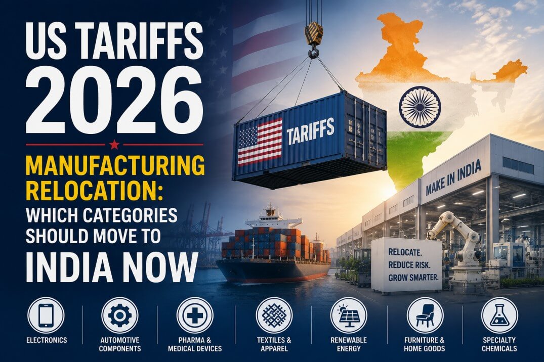
Green Manufacturing and Scope 3 Emissions: How India Sourcing Reduces Your Supply Chain Carbon Footprint

Introduction

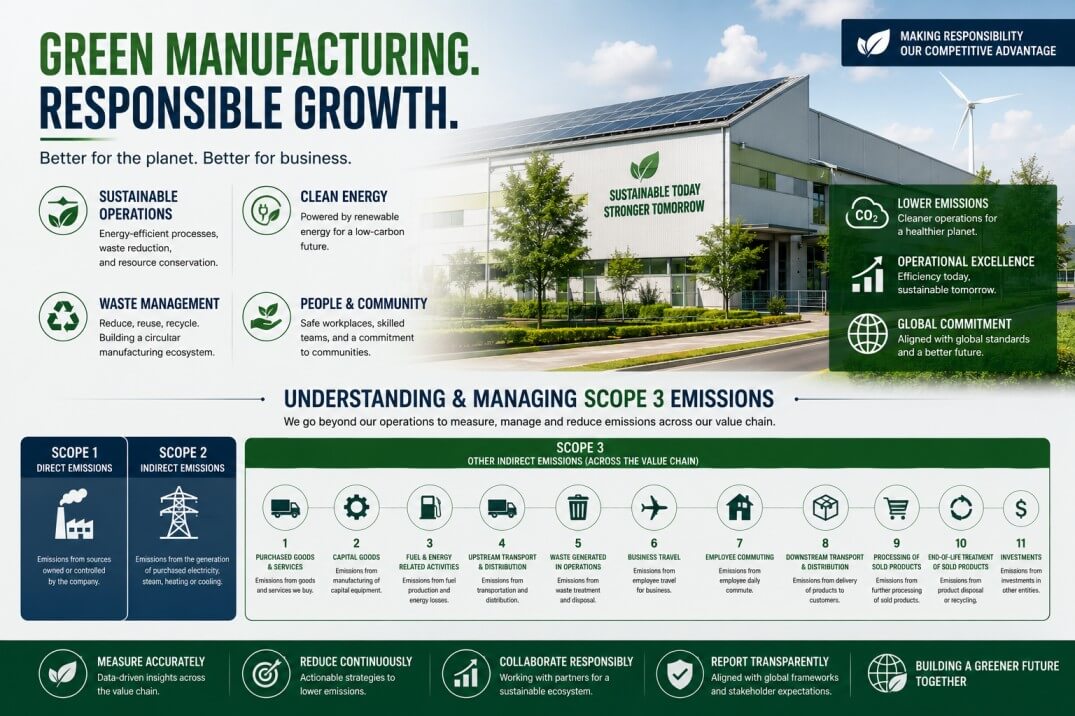
In 2026, Scope 3 supply chain emissions are no longer a sustainability report footnote – they are a procurement criterion, an investor disclosure requirement, and an increasingly literal cost under the EU Carbon Border Adjustment Mechanism (CBAM). For manufacturing companies with net-zero commitments or EU export programmes, the carbon intensity of their supply chain – including the electricity used to manufacture their components – now affects both compliance and cost.

India’s energy transition, combined with its lower-carbon manufacturing profile versus China for specific categories, makes it an increasingly relevant variable in Scope 3 reduction strategy. This article gives procurement and sustainability teams the data they need.

Why Manufacturing Location Affects Scope 3 Emissions

Scope 3 emissions (Category 1: Purchased Goods and Services) are dominated by:

  • Electricity used in manufacturing (grid emission factor of supplier country/region)
  • Process energy (thermal – coal, gas, oil for furnaces, dryers, kilns)
  • Logistics emissions (shipping mode and distance)
  • Material extraction and processing (upstream Scope 3)

The single largest variable is grid electricity carbon intensity – the kg of CO2 equivalent emitted per kWh consumed. This varies dramatically by country:

  • China national grid average (2025): 0.581 kg CO2e/kWh (coal-heavy grid)
  • India national grid average (2025): 0.472 kg CO2e/kWh (improving with renewable additions)
  • India Tamil Nadu / Rajasthan grid (high-renewable zones): 0.320-0.380 kg CO2e/kWh
  • India industrial parks with captive solar/wind: 0.150-0.250 kg CO2e/kWh
  • EU average: 0.233 kg CO2e/kWh
  • US average: 0.371 kg CO2e/kWh

For an energy-intensive manufacturing process consuming 500 kWh per tonne of output, switching from China to a renewable-powered India industrial park reduces electricity-related Scope 3 emissions by 40-70%.

India’s Renewable Energy Transition: The Manufacturing Implication

India reached 200 GW of installed renewable energy capacity in 2024 and is targeting 500 GW by 2030. In manufacturing terms, this means:

  • Multiple states (Tamil Nadu, Rajasthan, Gujarat, Karnataka) now have renewable energy surplus – enabling genuine green power procurement for industrial consumers.
  • Open Access renewable power (directly contracted with generators) is available in most major manufacturing states, enabling manufacturers to lock in low-carbon power at 20-30% lower tariff than grid power.
  • Government industrial parks in renewable-energy-rich states offer pre-built renewable supply infrastructure – buyers can specify “green-powered facility” in RFQs.
  • India’s national green energy grid corridor investment (Rs 20,440 Cr) is enabling interstate renewable power transfers, democratising access to green power.

Carbon Border Adjustment Mechanism (CBAM) and India Sourcing

The EU’s CBAM, fully phased in from January 2026, applies a carbon price to embedded emissions in imports of steel, aluminium, cement, fertilisers, hydrogen, and electricity from non-EU countries. Importers must purchase CBAM certificates matching the carbon price they would have paid under EU ETS.

India vs China CBAM comparison for steel products (illustrative):

  • China steel production: Approximately 2.0-2.4 tonnes CO2e per tonne of steel (blast furnace, coal-based)
  • India steel production (DRI/EAF route, Tata Steel, JSW): Approximately 1.4-1.8 tonnes CO2e per tonne
  • India steel with green hydrogen DRI (pilot projects in 2026): Below 0.5 tonnes CO2e per tonne (emerging)
  • At an EU ETS carbon price of 80 EUR/tonne CO2, the CBAM cost difference between India and China steel can reach 48-80 EUR per tonne – a significant landed cost variable for steel-intensive products.

Building a Green Supply Chain with India Sourcing

Step 1: Measure Current Scope 3 Baseline

Before optimising, measure. Calculate Scope 3 Category 1 emissions using your current China supplier spend data: tonnes of product x emission factor (kg CO2e/kg for typical material and process). Primary sources: supplier-provided EPD (Environmental Product Declaration), IPCC emission factors, or Ecoinvent database.

Step 2: Identify High-Emission, India-Substitutable Categories

Rank your BOM by: Scope 3 emission intensity (kg CO2e/$ spend) x substitutability with India supplier. High-emission, India-substitutable categories include: steel forgings and castings, aluminium die castings, precision machined steel components, and electronics assemblies.

Step 3: Specify Green Criteria in India RFQs

Include in your RFQ: request for supplier’s power purchase agreement (PPA) documentation for renewable energy, electricity consumption per unit of output (allows you to calculate Scope 3 reduction), and supplier’s annual GHG inventory (if available). Prefer suppliers in Tamil Nadu, Rajasthan, and Gujarat industrial parks with documented green power access.

Step 4: Claim and Report the Reduction

Document the emission factor of your India supplier vs previous China supplier. Report the reduction as Category 1 Scope 3 improvement under GHG Protocol. Quantify the avoided carbon cost under CBAM or internal carbon pricing frameworks.

Indian Certifications Relevant to Green Manufacturing

  • BEE (Bureau of Energy Efficiency) Star Rating: Indian energy efficiency certification for industrial facilities. Higher star rating = lower energy intensity.
  • GreenPro Certification (CII): Indian green product certification for manufactured goods, covering lifecycle emissions, water use, and hazardous substance content.
  • ISO 14001 (Environmental Management System): International standard; widely held by export-oriented Indian manufacturers. Verifies systematic approach to environmental management.
  • Carbon Disclosure Project (CDP) Supply Chain: Increasingly adopted by large Indian manufacturers supplying to global companies with CDP commitments.

Key Takeaways

  • India’s grid carbon intensity is 19% lower than China’s national average and improving rapidly with renewable additions.
  • India industrial parks with captive solar/wind power offer emission factors 60-70% below China’s coal-heavy grid.
  • EU CBAM creates a direct financial incentive to source steel and aluminium from lower-carbon India manufacturers vs high-carbon Chinese equivalents.
  • Specifying renewable energy access and ISO 14001 in India RFQs is achievable and increasingly standard practice for export-oriented Indian manufacturers.
  • Scope 3 Category 1 reduction from India sourcing can be material (20-40% per component category) and directly reportable under GHG Protocol.

FAQ

Q: How do I get verified emission data from an Indian supplier for Scope 3 reporting?

A: Request an Environmental Product Declaration (EPD) if the supplier has one. If not, request electricity consumption per unit of output + power purchase documentation. Use the electricity data with CEA (Central Electricity Authority) India published grid emission factors by state to calculate Scope 3 emissions. For higher precision, engage a third-party carbon accounting firm to conduct a supplier-specific LCA.

Q: Does sourcing from India count as “domestic” for US IRA manufacturing content requirements?

A: No. US IRA domestic content requirements specify US-origin manufacturing for maximum incentives. India is not a free trade agreement partner with the US (as of 2026, although negotiations are advancing). For IRA compliance, India sourcing does not qualify for domestic content bonuses but does benefit from standard MFN tariff treatment vs China’s Section 301 tariff surcharges.

Q: What is the carbon footprint of shipping goods from India vs China to the US?

A: India to US East Coast by sea: approximately 18-22 days transit, ~0.010-0.012 kg CO2e per tonne-km (Maersk Emission Factor 2025). China to US West Coast: approximately 14-16 days, similar emission factor. The difference in logistics emissions between India and China sourcing is small relative to the manufacturing process emission difference – typically less than 5% of total supply chain carbon.

Injection Moulding in India: Complete Guide to Plastic Part Manufacturing and Sourcing

Introduction

India processes over 12 million tonnes of plastic annually and has more than 30,000 plastics processing units. Yet most global buyers sourcing injection moulded parts default to China without evaluating India – leaving 20-35% cost savings on the table for non-cosmetic, industrial, and automotive plastic parts where India is genuinely competitive. This guide maps India’s injection moulding ecosystem, what it can and cannot do, how to specify parts correctly, and how to qualify Indian moulders for global supply programmes.

India’s Injection Moulding Ecosystem: Capabilities and Clusters

Automotive Plastic Components – Mature and Export-Ready

India’s automotive plastic parts industry supplies to Maruti Suzuki, Hyundai, Tata Motors, and through tier-1 suppliers (Motherson, Faurecia India, Pricol, Varroc) to global automotive OEMs. Capabilities include: instrument panels, door trim assemblies, bumper systems, fuel system components, under-hood parts in PA66, PBT, and HDPE. IATF 16949-certified moulders are the norm for automotive.

Industrial and Engineering Plastics – Growing

Engineering plastic moulding (PA, POM, PPS, PEEK, PEI) for industrial applications: pump housings, valve bodies, bearing retainers, conveyor components, and electrical enclosures. Manufacturers in Pune, Ahmedabad, and Bengaluru handle engineering plastics with in-house tool rooms.

Consumer Electronics and Appliance Components – Competitive for Functional Parts

India moulders produce functional enclosures, connectors, and internal components for consumer electronics assembled in India (primarily for Foxconn, Tata, and Samsung’s India operations). For Class-A cosmetic surface finish consumer products (phone casings, premium appliance aesthetics), China remains ahead on mould polish quality and cycle time.

Medical Device Components – Developing

ISO 13485-certified injection moulding for medical grade plastics (HDPE, PP, ABS, PC, PSU, PEEK) is growing. Cleanroom moulding facilities (ISO Class 7/8) are available in Pune, Hyderabad, and Chennai. India Medical Device Rules (MDR 2017) compliance is the regulatory framework for India-market devices; for export programmes, FDA 21 CFR Part 820 or EU MDR compliance is required.

Tooling (Mould) Costs in India vs China

Tooling cost comparison for a typical single-cavity injection mould:

  • Simple part (no lifters, 2-plate tool): China $2,500-6,000 | India $3,500-8,000
  • Medium complexity (4-plate, slides): China $8,000-20,000 | India $10,000-25,000
  • Complex part (hot runner, multiple slides, high polish): China $20,000-60,000 | India $28,000-80,000
  • Multi-cavity mould (8-cavity, standard): China $12,000-30,000 | India $15,000-38,000

India’s tooling cost premium over China is 20-35%. However, for programmes where the buyer intends to keep tooling in India (for supply chain security, tariff avoidance, or import duty reasons), the tooling premium is a one-time cost recovered quickly through lower unit prices.

Unit Cost Comparison: When India Is Cheaper

India moulding unit costs are competitive vs China for:

  • Parts with high assembly labour content (insert moulding, overmoulding): India wins by 25-35%
  • Large structural/industrial parts (wall thickness above 3mm, high shot weight): India competitive within 10%
  • Low-to-medium cavitation tools (1-4 cavity): India competitive
  • Engineering plastics with manual insert loading: India wins by 20-30%

India is less competitive than China for:

  • Ultra-high-cavitation moulds (16+ cavity, thin-wall consumer packaging): China’s mould precision and cycle time optimisation is superior
  • Class-A cosmetic finishes for consumer electronics: Chinese mould polishing and EDM texture capability is ahead
  • Very high volumes requiring 24/7 automated cells: China’s automation investment is greater

DfM Rules for India Injection Moulding: What to Check Before Tooling

Wall Thickness

Uniform wall thickness is the single most important DfM rule. Nominal wall should be 2-4mm for most engineering plastics. Variation greater than 25% from nominal creates sink marks and warpage. For thin-wall moulding (below 1.5mm), specify to moulders with documented thin-wall experience.

Draft Angles

Minimum 1 degree draft on all vertical walls for easy ejection. Textured surfaces require 3-5 degrees. Insufficient draft causes drag marks and ejection damage – the most common DfM mistake from engineers who work in metals.

Gate Location

Gate location affects weld line position, surface finish, and filling pressure. Work with the moulding supplier on gate location during DfM review – before tooling is cut. Moving a gate after tool fabrication is costly.

Undercuts

Undercuts require side actions (slides or lifters) which add $500-5,000 per action to tooling cost. Redesign to eliminate undercuts where possible; if unavoidable, call them out explicitly in the design review.

Sink Marks and Boss Design

Boss wall thickness should be 60-70% of nominal wall. Ribs should be 40-60% of nominal wall. Exceeding these ratios creates sink marks on the opposite face. This is a non-negotiable rule for appearance surfaces.

Quality Standards for Injection Moulded Parts in India

  • Automotive: IATF 16949 (quality management system), customer-specific requirements (VDA 6.3 for VW-group, AIAG PPAP for US OEMs)
  • Industrial: ISO 9001 as minimum; EN/ISO 10350 for material property verification
  • Medical: ISO 13485, cleanroom certification per ISO 14644, material biocompatibility per ISO 10993
  • Electronics: IEC 60695 (flammability), UL 94 rating on resin selection
  • Food-contact: FDA 21 CFR food contact approval on resin, EU 10/2011 migration testing

How to Qualify an India Injection Moulding Supplier

Toolroom Assessment

Visit or audit the in-house tool room (or confirm tool shop relationship for outsourced tooling). Check: CNC machining and EDM equipment (age, maintenance), mould steel standard used (P20, H13 for standard tools; S136, 420 SS for corrosive resins), mould flow simulation capability (Moldflow or equivalent).

Press Fleet Assessment

Injection moulding presses are rated by clamping force (tonnes). Check: press fleet size and age (equipment under 10 years preferred), clamping force range (needs to match your part projected area), process controls (closed-loop pressure/velocity, temperature controllers), maintenance records.

Material Management

Verify: incoming material inspection (MFR/viscosity testing on each lot), drying equipment (dehumidifying dryers for hygroscopic resins: PA, PC, PET, PBT), material traceability to lot number, segregation of medical-grade vs industrial-grade resins.

Key Takeaways

  • India is cost-competitive for injection moulding in automotive parts, industrial engineering plastics, and labour-intensive assemblies (insert moulding, overmoulding).
  • India’s tooling costs are 20-35% higher than China but recovered through lower unit costs on medium-to-high volume programmes.
  • China retains an advantage for Class-A cosmetic consumer electronics and ultra-high-cavitation thin-wall packaging.
  • DfM review before tooling – specifically wall thickness, draft, gate location, and undercuts – is the single highest-leverage quality intervention.
  • India has IATF 16949, ISO 13485, and ISO 9001-certified moulders for automotive, medical, and industrial programmes respectively.

FAQ

Q: Can India moulders handle overmoulding (TPE over rigid substrate) and 2K moulding?

A: Yes – multiple India moulders have 2K (two-component) and overmoulding capability for automotive soft-touch interiors, industrial grips, and sealing applications. Specify 2K capability explicitly in your RFQ and request reference parts during qualification.

Q: How do I specify colour matching for injection moulded parts from India?

A: Specify Pantone or RAL colour reference. Require colour master approved prior to production (limit sample process). Specify Delta-E tolerance (typically Delta-E below 1.0 for automotive, below 2.0 for industrial). Request colour control plan from the supplier showing measurement frequency and instrument (spectrophotometer).

Q: What import duties apply to India-origin plastic parts entering the US and EU?

A: Most injection moulded plastic components from India enter the US at standard MFN duty rates of 2.5-6.3% depending on HTS code – far below the 25%+ Section 301 rates applying to Chinese-origin equivalents. EU-India FTA negotiations in 2025-2026 are expected to further reduce or eliminate duties on Indian-origin manufactured goods.

Forging vs Casting: How to Choose the Right Metal Forming Process for Your Part

Introduction

Forging and casting are both net-shape or near-net-shape metal forming processes – but they produce fundamentally different internal structures, mechanical properties, and cost profiles. A crankshaft that should be forged but is cast will fail prematurely. A complex valve housing that should be cast but is specified for forging will cost 3x more than necessary. The process selection decision is one of the highest-leverage engineering choices in metal part design.

This guide gives you a systematic framework for choosing between forging and casting based on the factors that determine part performance and cost: mechanical properties, geometry, material, volume, and application criticality.

Process Overview

Forging

Forging applies compressive force to a heated metal workpiece – using hammers, presses, or rolls – to shape it while simultaneously improving its internal grain structure. The forging process works the metal, breaking up porosity, aligning grain flow with part geometry, and producing a dense, directionally-strong microstructure.

Process variants: Open-die forging (large, simple shapes), closed-die forging (complex net-shape parts in a die), ring rolling (rings and flanges), roll forging (bars and rods).

Casting

Casting pours molten metal into a mould and allows it to solidify. The mould defines the part geometry; the metal fills complex cavities that would be impossible to forge. Casting produces a randomly-oriented grain structure with some inherent porosity risk, but enables geometrical complexity that forging cannot achieve.

Process variants: Sand casting (large parts, low tooling cost), investment casting (complex geometry, excellent surface finish), die casting (high-volume non-ferrous), lost-foam casting.

Mechanical Properties: The Most Critical Difference

This is where forging wins decisively. The forging process produces:

  • Grain flow aligned to part geometry: In a forged crankshaft, grain lines follow the contour of the pin journals and web, maximising fatigue resistance along stress paths. A cast crankshaft has random grain orientation.
  • Higher strength and toughness: Forged steel typically achieves 20-30% higher yield strength and 30-50% higher fatigue life than equivalent cast steel at the same alloy and heat treatment.
  • No porosity: Forging works out internal voids. Casting always carries some porosity risk (managed with process control, but never eliminated).
  • Better impact resistance: Forged parts absorb impact energy through plastic deformation before fracture; cast parts tend to fracture more abruptly.

Practical consequence: Any part that carries cyclic loading (fatigue), impact loads, or safety-critical stress must be forged. Any part where weight reduction per unit strength is the design goal should be forged.

Head-to-Head Comparison

  • Mechanical Strength: Forging – Superior (20-30% higher UTS vs cast equivalent) | Casting – Good (adequate for many applications)
  • Fatigue Life: Forging – Very High (grain flow alignment) | Casting – Moderate (random grain, porosity risk)
  • Porosity: Forging – None (compressive process eliminates voids) | Casting – Present (managed but inherent)
  • Geometry Complexity: Forging – Limited (parting line constraint, no internal cavities) | Casting – Excellent (internal passages, complex 3D geometry)
  • Material Range: Forging – Steel, aluminium, titanium, nickel alloys | Casting – Virtually any metal including superalloys
  • Surface Finish (as-formed): Forging – Moderate (Ra 3.2-6.3 micron) | Casting – Good (investment: Ra 1.6-3.2 micron)
  • Dimensional Tolerance (as-formed): Forging – Medium (+/- 0.5-2mm) | Casting – Better for investment (+/- 0.1-0.25mm)
  • Tooling Cost: Forging – High ($20,000-200,000 for closed-die) | Casting – Medium-Low ($3,000-50,000)
  • Unit Cost (volume): Forging – Low at high volume | Casting – Low to medium
  • Best Volume: Forging – 5,000-1,000,000+ units/year | Casting – 100-500,000 units/year

When to Use Forging

Forging is mandatory or strongly preferred when:

  • Part carries cyclic/fatigue loading: crankshafts, connecting rods, wheel hubs, axle shafts, gear blanks, surgical implants, aircraft structural components
  • Part must not fail catastrophically: safety-critical fasteners, aircraft landing gear, engine connecting rods, suspension knuckles
  • High strength-to-weight ratio is required: aerospace structures, race car components, high-performance automotive parts
  • Impact resistance is critical: hand tools, mining equipment, off-highway vehicle components
  • The geometry can be formed with simple parting lines and no internal cavities

When to Use Casting

Casting is preferred when:

  • Part has complex internal geometry: valve bodies with multiple ports, pump casings with internal volutes, turbine blades with internal cooling channels
  • Material is a superalloy, cast iron, or titanium alloy where forging is impractical or prohibitively expensive
  • Volume is below the threshold for forging die amortisation (typically below 5,000 units/year)
  • Part is structural/static with no fatigue loading: brackets, housings, manifolds, frames
  • Near-net shape with tight tolerances is required without post-machining: investment cast valve bodies at +/- 0.15mm

Material-Process Compatibility

Aluminium Alloys

Both forging (6061-T6, 7075-T6) and casting (A356, A380 die cast) are mature. Forged aluminium is preferred for structural aerospace and automotive (wheels, suspension). Cast aluminium dominates for housings, engine blocks (die cast), and decorative applications.

Steel and Alloy Steels

Steel forgings (4140, 4340, 8620) are the backbone of automotive and industrial power transmission. Cast steel (investment cast or sand cast) handles complex housings and valve bodies. Cast iron (grey, ductile) remains dominant for engine blocks, brake discs, and machine beds – rarely forged.

Titanium

Titanium forging (Ti-6Al-4V) is standard for aerospace structural components (frames, fasteners, landing gear). Titanium casting (investment cast) handles complex aerospace fittings and biomedical implants. Both require inert atmosphere or vacuum to prevent oxidation during processing.

Nickel Superalloys

Nickel superalloy forgings (Inconel 718, Waspaloy) are used for turbine discs, compressor blades, and high-temperature structural parts. Nickel superalloy castings (investment cast) produce turbine blades with cooling channels. These are complementary – turbine disc = forged; turbine blade = investment cast.

India’s Forging and Casting Ecosystem

India is the world’s second-largest forging industry (after China) with annual output exceeding $5B. Rajkot is Asia’s largest forging cluster. Pune, Aurangabad, and Ludhiana are major secondary clusters. Key capability: steel forgings for automotive (crankshafts, connecting rods, axle beams, flanges), industrial (flanges, fittings), and oil and gas (pressure vessel components, pipeline fittings).

India’s casting industry is also globally significant, with investment casting, sand casting, and die casting capabilities in Coimbatore (pumps, compressors), Rajkot (valves, fittings), Pune (automotive castings), and Kolkata (heavy castings). Indian investment castings supply aerospace and defence OEMs globally.

Key Takeaways

  • Choose forging for fatigue-loaded, impact-resistant, safety-critical parts where grain flow alignment and absence of porosity are functional requirements.
  • Choose casting for geometrically complex parts, superalloy and cast iron materials, lower volumes, and applications where geometry cannot be achieved by forging.
  • Forging produces 20-30% higher strength at equivalent alloy and heat treatment – this is a structural property advantage, not just a process preference.
  • India is the world’s second-largest forging industry with a mature export base: Rajkot, Pune, and Ludhiana clusters supply global automotive and industrial OEMs.
  • The forging vs casting decision should be made during design – switching processes after tooling investment is expensive and disruptive.

FAQ

Q: Can a part be designed for forging and then switched to casting to save money?

A: Only if the application does not require forging’s mechanical properties. Switching a fatigue-loaded part from forging to casting to save tooling cost is a safety risk – casting will have lower fatigue life. For non-fatigue-loaded structural parts (brackets, housings), switching can be economical if geometry is compatible.

Q: What is the typical tooling cost difference between forging and investment casting?

A: Closed-die forging tooling: $20,000-200,000 depending on part complexity and material. Investment casting wax die tooling: $3,000-30,000. The tooling cost gap means casting is more economical below approximately 5,000-10,000 units/year; above that volume, forging’s lower unit cost makes it preferable for compatible geometries.

Q: How do I specify forging quality on a drawing?

A: Key specifications: material grade and heat treatment (e.g., AISI 4340, quench and temper to 40-45 HRC), forging grain flow direction (specify if critical), forging class (per ASTM A788 or equivalent), Charpy impact test if required, ultrasonic testing for internal discontinuities per ASTM A388, and dimensional tolerances per DIN 7526 or equivalent forging tolerance standard.

Wire Harness Manufacturing in India: Cost Advantage, Capability, and Supplier Qualification Guide

Introduction

Wire harness manufacturing is the most labour-intensive sub-assembly in automotive and industrial manufacturing. A single passenger vehicle contains 1-3 km of wiring and 500-2,000 electrical connections. At $15-80 per harness (automotive), labour represents 55-65% of total cost. This makes wire harness manufacturing the category where India’s labour cost advantage is most decisive – and why India is already the world’s third-largest wire harness exporter, supplying to Toyota, Honda, Volkswagen, and General Motors assembly lines globally.

This guide covers India’s wire harness manufacturing ecosystem, cost benchmarks, quality standards, supplier qualification, and how to establish India sourcing for harness programmes in 2026.

Why Wire Harnesses Are India’s Strongest Contract Manufacturing Advantage

Wire harness assembly is fundamentally a hand-work intensive process. Automated assembly covers crimping, cutting, and terminal insertion but cannot fully automate the routing, binding, labelling, and quality inspection steps that make harnesses complex. The labour content cannot be automated away – which means the country with the lowest skilled-labour cost wins permanently.

Labour cost comparison for wire harness assembly (2026 estimates):

  • China (coastal): $3.80-5.20/hour for harness assembler
  • Mexico: $4.50-6.00/hour
  • Eastern Europe (Romania, Poland): $7.00-11.00/hour
  • India (Tier-1 cities): $1.00-1.60/hour
  • India (Tier-2 cities – Hosur, Pune, Nashik): $0.75-1.20/hour

For a harness with 4 hours of assembly labour, India saves $10-16 per unit versus China and $24-40 per unit versus Eastern Europe. At 100,000 units/year, that is $1-4M in annual savings.

India’s Wire Harness Manufacturing Ecosystem

Tier-1 Global Suppliers with India Manufacturing

Motherson Sumi Systems (now Samvardhana Motherson International) is the world’s largest wire harness manufacturer by revenue and operates multiple India plants supplying Toyota, Volkswagen, and Honda globally. Pricol Technologies, Minda Industries, and Spark Minda supply domestic OEMs (Maruti Suzuki, Tata Motors, Mahindra) and export harnesses to Europe and Japan.

Contract Manufacturers for Non-Automotive Harnesses

India has a significant mid-tier harness manufacturing base for industrial, aerospace, defence, and consumer electronics applications. Companies in Pune, Bengaluru, Hosur, and Chennai manufacture harnesses to IPC-A-620 (wiring harness workmanship), DEF STAN, and customer-specific standards. These are the relevant suppliers for non-automotive buyers.

Key Manufacturing Clusters

  • Pune / Nashik: Automotive wire harness hub; Motherson, Minda, tier-2 suppliers
  • Chennai / Hosur: Auto and electronics harness manufacturing
  • Bengaluru: Aerospace and defence harness manufacturing (AS9100 certified suppliers)
  • Noida / Gurugram: Industrial and commercial harness manufacturing

Quality Standards for Wire Harnesses: What to Specify

IPC-A-620 (Acceptability of Cable and Wire Harness Assemblies)

The primary quality standard for wire harness workmanship. Specifies acceptability criteria for soldering, crimping, routing, bundling, labelling, and connector insertion. Three classes: Class 1 (general electronics), Class 2 (dedicated service), Class 3 (high-reliability aerospace/defence). Always specify IPC-A-620 Class in your purchase specification and verify supplier holds current IPC Certified Interconnect Specialist (CIS) certification.

USCAR-2 (Automotive Wire Crimp Performance Standard)

The automotive-specific crimp performance standard specifying pull force, cross-section, and electrical resistance requirements for crimped terminals. Required for any automotive-grade harness. Indian automotive harness manufacturers supplying to global OEMs hold USCAR-2 compliance as a baseline requirement.

IPC-J-STD-001 (Soldering)

For harnesses with soldered connections (junction blocks, pigtails, tinned end splices). Specifies soldering materials, flux residue, and inspection criteria. J-STD-001 Class 3 for aerospace/defence, Class 2 for industrial.

AS9100 (Aerospace Wire Harnesses)

Any wire harness destined for aerospace or defence applications requires AS9100 Rev D supplier certification as a minimum. India has AS9100-certified harness manufacturers in Bengaluru and Pune.

The Wire Harness Supplier Qualification Process

Step 1: Define Specification Package

Before issuing RFQs, prepare: harness drawing (or 3D cable design file), wire gauge and material specification, connector part numbers (with AMP/Molex/TE Connectivity or equivalent), environmental requirements (temperature, vibration, IP rating), quality standard (IPC-A-620 Class), testing requirements (hipot, continuity, resistance).

Step 2: RFQ and Supplier Selection

Issue to minimum 3 India suppliers. Evaluate: current customer list (who else do they supply and at what quality level), certification status (IPC-A-620, IATF 16949, AS9100 as applicable), tooling capabilities (crimp press inventory, test equipment), and capacity availability.

Step 3: First Article and Process Qualification

First article inspection (FAI) per harness drawing. 100% dimensional and electrical check on first articles. Review process documentation: work instructions, crimp force monitoring records, operator certifications. Approve process before volume production begins.

Step 4: Production Approval and Ongoing Quality

Issue production purchase order with: AQL sampling plan for ongoing inspection, monthly quality scorecards (PPM defect rate, on-time delivery), annual process audit. India suppliers should achieve PPM below 500 for established programmes; world-class is below 50 PPM.

Lead Times and Logistics for India-Sourced Wire Harnesses

Standard production lead time from approved supplier: 4-6 weeks for standard programmes, 8-12 weeks for new programme with tooling. First article lead time from drawing release: 3-4 weeks.

Logistics: Wire harnesses are high-volume, low-density (bulky, light). Sea freight is preferred for annual programmes. India to US East Coast: 22-26 days. India to Europe: 16-20 days. For automotive JIT supply, airfreight supplements during ramp-up or expedites. Consider India-based bonded warehousing for volume programmes to reduce effective lead time to 1-2 weeks.

Cost Benchmarking: What to Expect from India Quotes

For a representative automotive door harness (40 circuits, 2.2m length, 180 terminals, USCAR-2 qualified):

  • China quote (Tier-2 manufacturer): $22-28 per assembly
  • Mexico quote (Tier-2 manufacturer): $26-34 per assembly
  • India quote (Tier-2 manufacturer): $14-19 per assembly

India is 30-40% cheaper than China on unit price before tariffs. With 25% Section 301 tariffs on Chinese wire harnesses, India’s landed cost advantage in the US market exceeds 50%.

Key Takeaways

  • Wire harness manufacturing is the highest-ROI India sourcing category: 30-40% lower unit cost than China, zero tariff exposure, established ecosystem.
  • India has tier-1 global harness manufacturers (Motherson) and a deep tier-2 contract manufacturing base for custom programmes.
  • IPC-A-620 (workmanship), USCAR-2 (automotive crimp), and AS9100 (aerospace) are the relevant quality standard triplet to specify.
  • Qualification from RFQ to first article approval: 6-10 weeks for standard harnesses.
  • India harnesses are not just cheaper – India’s established global automotive customer base (Toyota, VW, Honda) validates quality at production scale.

FAQs

Q: Can India suppliers handle complex aerospace wire harnesses with shielding, backshell connectors, and MIL-spec wire?

A: Yes – Bengaluru and Pune have AS9100-certified harness manufacturers experienced in MIL-W-22759 wire, MIL-C-26482 connectors, EMI backshell, and coaxial harness assemblies. Reference programmes include supply to Airbus, HAL, and DRDO. Qualification of a new aerospace harness programme typically takes 9-15 months including DFM, FAI, and first-flight approval.

Q: What is the minimum order quantity for India wire harness sourcing?

A: For custom harnesses, minimum economic order is approximately 500 pieces/year. Below that, tooling amortisation (crimp tooling, test fixture) makes India less competitive than domestic assembly. For standard harness assemblies using off-the-shelf connectors, even smaller quantities are viable.

Q: How do I manage harness design changes in an India-sourced programme?

A: Establish a formal engineering change control process with your India supplier: all drawing changes go through a change note with FAI trigger for dimensional or electrical changes. India suppliers with automotive experience have mature ECN processes. Budget 2-3 weeks for FAI on significant changes.

EV Manufacturing in India 2026: Battery Supply Chain, PLI Incentives, and OEM Entry Guide

Introduction

India’s electric vehicle transition has entered its industrial phase in 2026. Installed EV production capacity has crossed 2 million units per year. Battery cell manufacturing facilities backed by PLI – including Ola Electric, Amara Raja, Exide Industries, and Reliance New Energy – are now producing cells. The EV PLI scheme has committed Rs 18,100 Cr to accelerate local production. Global OEMs including BYD, Hyundai, and Tesla are either building or evaluating India EV manufacturing facilities.

For global supply chain executives, India’s EV ecosystem in 2026 offers two distinct opportunities: sourcing EV components from India for global programmes, and establishing India manufacturing for the Indian EV market. This guide maps both.

India EV Market in 2026: The Context

India is now the world’s third-largest EV market by two-wheeler and three-wheeler volume and the sixth-largest by passenger car EV sales. Key 2026 data points:

  • Two-wheeler EVs: 5.2 million units sold annually (36% of total two-wheeler market)
  • Three-wheeler EVs: 800,000 units (58% of total three-wheeler market)
  • Passenger car EVs: 520,000 units (8.5% of passenger car market – growing rapidly)
  • Commercial EV (buses, LCVs): 85,000 units
  • Total EV penetration by volume: 28% of all vehicles sold

The government’s FAME III scheme (successor to FAME II) is driving commercial and public transport electrification. State EV policies in Tamil Nadu, Maharashtra, Telangana, and Gujarat offer additional incentives. India’s EV trajectory is not aspirational – it is happening at scale.

Battery Cell Manufacturing: What Is Operational in 2026

Ola Electric – Krishnagiri, Tamil Nadu

Ola Electric’s Gigafactory (Phase 1) is producing lithium-ion cells (NMC chemistry, 4680 form factor) with 5 GWh annual capacity in 2026, ramping to 100 GWh by 2030. This is India’s first indigenous cell manufacturing at volume. Ola is vertically integrated – cells to battery packs to two-wheeler production at the same campus.

Amara Raja Energy & Mobility – Divitipalle, Telangana

Amara Raja’s Giga Corridor (Phase 1 operational 2025-2026) produces LFP (Lithium Iron Phosphate) cells targeting two-wheelers, three-wheelers, and commercial vehicles. LFP chemistry offers superior thermal safety and cycle life – preferred for high-temperature Indian operating conditions.

Reliance New Energy – Jamnagar, Gujarat

Reliance’s solar-integrated battery manufacturing facility is ramping in 2026, targeting large-format cells for stationary storage and commercial EV applications. Partnership with lithium cell technology provider for transfer of advanced cell manufacturing know-how.

Exide Industries – Multiple Locations

Exide’s Li-ion cell plant is operational in 2026, leveraging its existing lead-acid battery manufacturing and distribution network. Focus on two-wheeler and compact passenger car battery packs.

The EV Component Supply Chain: Where India Is Competitive Now

Battery Packs (BMS + Modules + Cells + Housing)

India has competitive battery pack assembly capability. Multiple tier-1 battery pack manufacturers (Tata AutoComp, Exide, Amara Raja, Epsilon Advanced Materials) supply OEMs. The bottleneck was cell supply – increasingly resolved by 2026 domestic cell production.

Electric Motors (PMSM, BLDC, Induction)

India has strong motor manufacturing capability: Bharat Bijlee, Mahindra CIE, HELLA India, and multiple tier-2 manufacturers produce PMSM and BLDC motors for two-wheelers, three-wheelers, and light commercial EVs. For passenger car EV motors (higher torque, higher precision requirements), qualification is needed but capability exists.

Power Electronics (Inverters, OBCs, DC-DC Converters)

India’s power electronics supply chain for EVs is developing. Companies like Tata Elxsi (design), KPIT Technologies (embedded), and a growing base of hardware manufacturers are building inverter and onboard charger capability. This is the most underdeveloped tier of India’s EV supply chain – significant gap and opportunity.

EV Structural Components (Battery Enclosures, Chassis, Subframes)

India’s established metal fabrication, casting, and forging capabilities directly apply to EV structural components. Battery enclosures in aluminium (die cast) and steel (stamped) are being produced at Bharat Forge, Sandhar Technologies, and multiple tier-2 stamping companies. This is a high-confidence supply area.

Thermal Management Systems

Heat exchangers, cooling plates, and thermal interface materials for battery systems – India has cooling system manufacturing capability but EV-specific thermal management is a developing niche. Global tier-1 suppliers (Valeo, Hanon Systems) are establishing India manufacturing to serve local OEMs.

PLI for Advanced Chemistry Cell (ACC) Battery Manufacturing

The PLI for Advanced Chemistry Cell Battery Manufacturing scheme (Rs 18,100 Cr) committed in 2021 and now in active production phase offers:

  • Incentive: 18-20% on net sales of ACC batteries above base year production
  • Qualifying capacity: Minimum 5 GWh per beneficiary
  • Duration: 5 years of incentives
  • Approved beneficiaries: Ola Electric, Amara Raja, Reliance New Energy, Rajesh Exports (later variants)

PLI incentive effect: At 18-20% on net sales, ACC PLI dramatically changes the economics of India battery production versus imported cells – effectively subsidising the ~25-30% cost premium India cells currently carry over Chinese cells at equivalent energy density.

How Global OEMs Are Entering India EV Manufacturing in 2026

Tesla Model Y – Pune Production

Tesla’s India assembly operation in Pune (CKD initially, progressing to SKD and local content ramp) began in 2025. India-produced Model Y targets the domestic market and serves as Tesla’s first Asia-Pacific manufacturing outside China. Components are progressively localised through an active India supplier development programme.

BYD – Pune Manufacturing JV

BYD’s India JV with Megha Engineering has received government approval and site selection is underway for a greenfield EV manufacturing facility targeting 100,000 units/year at full ramp. BYD brings its Blade Battery technology; the India JV enables competitive local pricing without import duties.

Hyundai and Kia – Tamil Nadu EV Expansion

Hyundai’s IONIQ 5 and IONIQ 6 are assembled at the Sriperumbudur plant with progressive localisation. Hyundai is the highest-volume premium EV player in India’s passenger car segment in 2026.

Key Takeaways

  • India’s EV transition is industrial-phase in 2026: cell manufacturing is operational, OEM assembly is scaling, and the supply chain is developing rapidly.
  • Battery cells, motor assemblies, structural components, and battery pack integration are India’s strongest EV supply chain capabilities in 2026.
  • Power electronics (inverters, OBCs) is the key supply chain gap – also the highest-margin opportunity for component manufacturers entering India.
  • PLI for ACC battery manufacturing (Rs 18,100 Cr) is actively disbursing and making India-produced cells increasingly cost-competitive.
  • Global OEMs establishing India EV manufacturing in 2026 are accessing one of the world’s fastest-growing EV markets with a full domestic supply chain advantage.

FAQ

Q: Are India-produced EV batteries competitive with Chinese cells on cost?

A: Not yet on pure cell-level cost – Chinese CATL and BYD Blade cells remain 15-20% cheaper at equivalent energy density. However, PLI incentives (18-20% on net sales), import duty savings, and logistics cost advantages make India-origin cells increasingly competitive for India-market applications and for export programmes where China-origin supply carries tariff exposure.

Q: What is the minimum order size for India EV component sourcing?

A: Battery pack integration: 500+ packs/year is commercially viable. Motor assemblies: 1,000+ units/year. Structural castings and stampings: 2,000+ units/year for economical tooling amortisation. Power electronics: most India suppliers are building capacity for 5,000+ units/year programmes.

Q: How does India EV manufacturing compare to China for export-oriented production?

A: India’s lower labour cost, zero-tariff access to US market (versus Chinese EVs facing 100%+ tariffs in 2026), and strengthening domestic supply chain make India increasingly competitive for export-oriented EV manufacturing targeted at the US, EU, and ASEAN markets.

India Semiconductor Manufacturing 2026: Fabs, OSAT, and the Supply Chain Opportunity

Introduction

In 2026, India’s semiconductor ambition has moved from policy document to construction site to operational facility. Micron’s OSAT plant in Sanand, Gujarat is packaging and testing DRAM and NAND chips. Tata Electronics’ semiconductor assembly and test facility in Jagiroad, Assam is operational. CG Power’s OSAT facility in Sanand is coming online. The Tata wafer fabrication facility in Dholera is in advanced construction. India is no longer a semiconductor aspiration – it is a semiconductor supply chain destination.

This article explains what is actually operational in 2026, what the capability boundaries are, what is coming in 2027-2028, and what it means for global electronics supply chains.

What Is Operational in India in 2026

Micron Technology – Sanand, Gujarat (OSAT)

Micron’s $2.75B OSAT (Outsourced Semiconductor Assembly and Test) facility began volume production in late 2025. The facility assembles and tests DRAM and NAND flash memory chips for global markets. At full ramp, it handles assembly, packaging, wafer probe, final test, and burn-in for memory devices destined for data centre, automotive, and consumer electronics applications.

Capability: Memory device OSAT only – DRAM and NAND. Not a logic or mixed-signal foundry. Capacity: ~450,000 wafer starts per month equivalent at full ramp. Strategic significance: This is the first major US semiconductor company to establish manufacturing in India.

Tata Electronics – Jagiroad, Assam (OSAT)

Tata’s first semiconductor facility, built in partnership with Powerchip Semiconductor Manufacturing Corporation (PSMC) of Taiwan, is operational for packaging and testing. The facility handles wafer bumping, flip-chip packaging, and test for mature-node logic chips and display drivers.

Capability: Mature-node chip packaging and test (28nm and above). Not a leading-edge logic fab. Capacity: Initial phase handling mid-tier volumes, ramping through 2026.

CG Power – Sanand, Gujarat (OSAT)

CG Power’s facility, developed in partnership with Renesas (Japan) and Stars Microelectronics (Thailand), focuses on automotive-grade and industrial semiconductor packaging. The facility targets IATF 16949-qualified automotive chip production – a critical gap given the 2021-2023 automotive chip shortage.

Capability: Automotive and industrial chip packaging (AEC-Q100 qualified). This is a strategically important capability differentiation.

The Dholera Fab: India’s First Wafer Fabrication Plant

Tata’s greenfield semiconductor wafer fabrication facility in Dholera Special Investment Region (Gujarat) – developed with PSMC – is under construction with first silicon expected in 2026-2027. Key parameters:

  • Node: 28nm and above (mature node) – not cutting-edge sub-5nm
  • Wafer size: 300mm
  • Target capacity: 50,000 wafer starts per month at full ramp
  • Target markets: Automotive ICs, power management, display drivers, microcontrollers, IoT devices
  • Investment: Rs 91,000 Cr (approximately $11B) with India Semiconductor Mission support

Strategic context: 28nm is the sweet spot for automotive, industrial, and consumer IoT applications. It is not competing with TSMC’s 3nm for AI chips – it is building India’s base in the semiconductor supply chain for the product categories India actually manufactures: cars, phones, industrial equipment.

What India’s Semiconductor Capability Means for Global Supply Chains in 2026

For Memory-Dependent Products: Immediate Benefit

Companies sourcing DRAM and NAND memory for products sold in the US or Europe can now specify India-origin packaging (Micron Sanand) to satisfy supply chain resilience and domestic content requirements. This is relevant for data centre equipment buyers, automotive electronics OEMs, and consumer electronics assemblers.

For Automotive Electronics: Emerging Benefit

CG Power’s Renesas-aligned OSAT provides AEC-Q100 qualified packaging for automotive chips. Companies building EV powertrains, ADAS systems, or vehicle body electronics who need to diversify away from Taiwan-concentrated automotive IC packaging have a new India option in 2026.

For Logic-Intensive Products (AI, High-Performance Computing): Not Yet

India has no leading-edge logic fab (sub-7nm). For AI accelerators, GPUs, and advanced mobile SoCs, TSMC Taiwan, Samsung Korea, and Intel Foundry remain the only options. India will not have leading-edge logic capability before 2030+ at the earliest.

The India Semiconductor Mission: Policy Support Through 2027

The India Semiconductor Mission (ISM) has committed Rs 76,000 Cr (approximately $9B) across three scheme windows:

  • Scheme A (Fab): 50% fiscal support for wafer fabrication facilities. Tata Dholera is the first beneficiary.
  • Scheme B (OSAT/ATMP): 50% fiscal support for assembly, testing, marking, and packaging. Micron, Tata, and CG Power are beneficiaries.
  • Scheme C (Compound Semiconductors/MEMS): 50% fiscal support for specialty semiconductor manufacturing. Several companies in advanced discussions.

The ISM has disbursed approximately Rs 18,000 Cr as of early 2026, with the remaining committed as facilities hit production milestones. The fiscal commitment is real and disbursed – not aspirational.

ECMS 2025 and the Component Ecosystem Around Semiconductors

The Electronics Component Manufacturing Scheme (ECMS 2025, Rs 22,919 Cr) targets the upstream component supply chain that semiconductor manufacturing requires: PCB substrates, advanced packaging materials, test socket components, and speciality chemicals. Several tier-1 component manufacturers from Japan, South Korea, and Taiwan have filed expressions of interest to establish India manufacturing under ECMS, attracted by PLI incentives and proximity to India’s growing semiconductor assembly base.

Key Takeaways

  • India has operational OSAT capability in 2026: Micron (memory), Tata Electronics (logic/display), and CG Power (automotive) are all producing.
  • Wafer fabrication (Tata Dholera, 28nm) is expected to yield first silicon in 2026-2027 – India is months, not years, away from domestic chip production.
  • India’s semiconductor capability is strongest in memory packaging, automotive-grade chips, and mature-node logic – the products that India’s growing electronics manufacturing base actually needs.
  • For leading-edge logic (AI chips, advanced mobile SoCs), India is not yet a supply option.
  • The India Semiconductor Mission’s Rs 76,000 Cr fiscal commitment is disbursing against production milestones – the money is real.

FAQ

Q: Can I source chips from India for my product in 2026?

A: For memory chips (DRAM, NAND): yes, Micron Sanand output. For automotive ICs (AEC-Q100): yes, CG Power Sanand. For general logic/microcontrollers from India-origin wafer fab: expected 2027+. For cutting-edge logic: not India in the foreseeable future.

Q: What does “OSAT” mean and how does it differ from a foundry?

A: A semiconductor foundry (like TSMC) fabricates chips from silicon wafers – it does the complex photolithography that creates transistors. An OSAT (Outsourced Semiconductor Assembly and Test) facility receives finished wafers from a foundry, cuts them into individual chips (dicing), packages them in protective housings, and tests them. India has OSAT facilities now; its first foundry is under construction.

Q: How does India semiconductor manufacturing interact with PLI for electronics?

A: India-origin components (including packaged semiconductors) can count toward domestic value addition requirements under PLI schemes, potentially increasing PLI incentives for electronics OEMs who source from Indian OSAT facilities. ECMS 2025 creates additional incentives for OSAT output consumed domestically.

US Tariffs 2026 and Manufacturing Relocation: Which Categories Should Move to India Now

Introduction

In 2026, the us tariff calculus for US importers has been reset again. The re-escalation of Section 301 tariffs under the new US trade policy framework – with effective rates on Chinese electronics now exceeding 145% on selected HTS codes – has eliminated the economics of China-origin sourcing across a broad set of product categories. The question facing every procurement team, CFO, and supply chain executive is no longer “should we diversify?” but “which categories should move now, to where, and how fast?”

This guide maps the highest-impact tariff categories, scores India’s readiness for each, and gives you a practical relocation decision framework for 2026.

The 2026 Tariff Landscape: What Changed

The 2025-2026 tariff escalation built on the Section 301 framework but added new product-level specificity. Key changes impacting manufacturing sourcing decisions:

  • Electronics and semiconductors: Effective rates on Chinese-origin electronics assemblies now range from 25% to 145% depending on HTS classification and product category.
  • Industrial machinery: Broad tariff application to CNC machine tools, motors, pumps, and compressors from China at 25% base rates.
  • Automotive components: 25% duties on most Chinese-origin auto parts, adding $300-800 per vehicle on China-sourced BOM.
  • Textiles and apparel: Sector-specific rates targeting garments, technical textiles, and industrial fabrics.
  • Medical devices: New tariff scrutiny on Class I and Class II Chinese-origin medical devices and sub-components.

The net effect: for any product where China-origin tariffs exceed 15-20%, the TCO advantage of Chinese manufacturing is partially or fully offset. At 25%+ tariffs, India is decisively cheaper on total landed cost for labour-intensive categories.

Category-by-Category Relocation Assessment

Electronics Assembly and EMS – Move Now

Tariff exposure: 25-145% on Chinese-origin electronics. India readiness: High. India’s EMS ecosystem (Foxconn, Tata Electronics, Jabil India, Zetwerk-network CMs) handles SMT assembly, system-level integration, and testing to IPC-A-610 Class 2/3 standards. Apple’s India-origin iPhone now accounts for over 18% of global production. The ecosystem is validated, scalable, and tariff-advantaged.

Decision: Immediate qualification of Indian EMS suppliers for any electronics assembly with 2026 China tariff exposure above 20%.

Wire Harnesses and Cable Assemblies – Move Now

Tariff exposure: 25% Section 301. India readiness: Very High. Wire harness manufacturing is the most labour-intensive automotive sub-assembly – and India’s wage advantage is most decisive here. Major automotive wire harness manufacturers (Motherson, Pricol, Minda) have established, export-oriented facilities. India is already a global wire harness export hub; the question is only supplier selection.

Forged and Cast Components – Move Now

Tariff exposure: 25% on most ferrous forgings and castings. India readiness: Very High. India is the world’s second-largest forging producer. Rajkot, Ludhiana, and Pune clusters supply European and US industrial OEMs. Investment casting, sand casting, and die casting ecosystems are export-mature. No ramp risk for qualified buyers.

Precision Machined Components – Move Now

Tariff exposure: 25% on most CNC-machined components. India readiness: High. Tier-2 and Tier-3 precision machining clusters in Pune, Coimbatore, and Bengaluru supply to aerospace, automotive, and industrial OEMs. AS9100, IATF 16949, and ISO 9001 certification coverage is strong.

Injection Moulded Plastic Parts – Move with Qualification

Tariff exposure: 25%. India readiness: Medium-High. India has a growing injection moulding industry but limited cosmetic-grade mould capability for consumer electronics. For industrial and automotive plastic parts, India is competitive. For high-gloss consumer-grade plastics, some tooling may still run in China with India assembly.

Semiconductor Devices – Move in 2-3 Years

Tariff exposure: Up to 145% on Chinese-origin semiconductors. India readiness: Developing. Micron’s OSAT facility in Gujarat (operational 2025) and Tata’s planned semiconductor fab (Dholera, 2026-2027) are progressing. OSAT and packaging is available now for qualifying programmes; full-stack fab capability is 2027+. For immediate needs, diversify to Taiwan, South Korea, and Malaysia for device sourcing.

Industrial Motors and Drives – Move with Qualification

Tariff exposure: 25%. India readiness: Medium. India has motor manufacturing capability (Bharat Bijlee, ABB India, Siemens India) but for custom specifications and specialised drive systems, qualification timelines of 6-12 months apply.

The 2026 Tariff-Adjusted TCO Model

Updating the TCO framework for 2026 tariff reality (representative electromechanical assembly, $500K annual spend):

China with 25% Section 301: Direct labour $180K + components $300K + logistics $22K + tariffs $125K + quality $12K = Total $654K

India with 0% tariff: Direct labour $72K + components $330K + logistics $20K + tariffs $0 + quality $10K = Total $450K

India TCO advantage: 31% lower landed cost. For HTS codes with 50%+ tariffs, India’s TCO advantage exceeds 45%.

How to Execute Relocation in 2026: A 90-Day Sprint

Days 1-15: BOM Triage

Pull every China-origin line item. Map each to its HTS code. Apply 2026 tariff schedule. Rank by: (annual China spend x tariff rate) to get dollar tariff exposure per part. This is your relocation priority list.

Days 15-45: Indian Supplier RFQ

For top 20% of tariff exposure (typically 80% of dollar impact), issue simultaneous RFQs to 3-5 Indian suppliers per category. Require: DFM review within 2 weeks, tooling quote within 3 weeks, first article timeline within 60 days of PO.

Days 45-75: Qualification

Run parallel India qualification against existing China production. FAI sign-off required before volume transfer. Do not cut China production until India qualification is complete and buffer stock covers lead time gap.

Days 75-90: Volume Transfer Plan

Commit volume transfer schedule. Build 8-12 weeks of India safety stock. Notify China suppliers of volume reduction with contractual notice period. Begin localising BOM where India-sourced components are available.

Key Takeaways

  • The 2026 tariff escalation has made China-origin sourcing economically indefensible for electronics, forgings, castings, precision machining, and wire harnesses.
  • India is the primary beneficiary: zero tariff exposure, established supplier ecosystem, and PLI-backed manufacturing investment.
  • The TCO advantage of India over China for tariff-exposed categories ranges from 25% to 45% on total landed cost.
  • The highest-readiness categories for immediate India sourcing are: EMS/electronics assembly, wire harnesses, forgings, castings, and precision machining.
  • A structured 90-day sprint can move the highest-tariff-exposure items to India qualification without production disruption.

FAQ

Q: Are the 2026 tariffs permanent or could they reverse?

A: The bipartisan consensus in the US on China trade policy makes full tariff reversal unlikely in any near-term scenario. Supply chain decisions made for 2026 should assume at least 3-5 year tariff persistence. The optionality cost of not diversifying – measured in tariff dollars paid – is higher than the qualification cost of India sourcing.

Q: Which Indian states offer the best incentives for manufacturing relocation investment?

A: Tamil Nadu (electronics, automotive), Gujarat (chemicals, semiconductors, EV batteries), Maharashtra (precision engineering, automotive), and Karnataka (aerospace, electronics) have the most active state-level incentive programmes in 2026, including land subsidies, power tariff concessions, and employment generation incentives layered on top of central PLI.

Q: How quickly can Indian suppliers be qualified for aerospace-grade components?

A: For AS9100-certified Indian suppliers with existing aerospace customer references, qualification timelines of 6-12 months are achievable for new Tier-2 components. First article inspection (FAI) and production part approval process (PPAP) are the primary timeline drivers.

Q: What about intellectual property risk in India vs China?

A: India is a common-law jurisdiction with robust IP protection mechanisms, a functioning court system for IP disputes, and TRIPS-compliant patent law. India’s IP risk profile is significantly lower than China for precision manufacturing, electronics, and pharmaceutical programmes.

Supply Chain Resilience: 10 Proven Strategies for Manufacturers in 2026

In 2021, a single semiconductor fabrication plant shortage grounded automotive production lines worldwide. In 2022, Shanghai lockdowns halted container shipping for weeks. In 2024, Red Sea disruptions added 10–14 days to Europe-Asia freight routes. In each case, the manufacturers who survived with the least damage were not the ones with the most efficient supply chains – they were the ones with the most resilient ones.

Supply chain resilience is no longer a nice-to-have in manufacturing strategy. It is the operating capability that determines whether disruption becomes a competitive advantage or an existential crisis.

What Is Supply Chain Resilience – and Why It Matters More Than Ever

Supply chain resilience is a supply chain’s capacity to anticipate disruptions, absorb them, and recover rapidly to normal performance – or, where possible, improve in the aftermath.

Resilience vs. Efficiency: The Trade-off Manufacturers Must Manage

Lean manufacturing and just-in-time supply chains optimise for efficiency: minimum inventory, minimum redundancy, maximum throughput. This efficiency comes at the cost of resilience. A supply chain with zero buffer inventory and a single source for every component is efficient – until a disruption hits, at which point it is fragile.

The question is not whether to be efficient or resilient – it is where to carry the resilience investment. The answer depends on the criticality of the component, the volatility of the supply base, and the cost of a production stoppage.

The Cost of Getting It Wrong: COVID-19, the Chip Shortage, and Beyond

The automotive semiconductor shortage of 2021 cost the global automotive industry an estimated USD 210 billion in lost revenue. Companies that had dual-source agreements or modest safety stock for critical semiconductors were back in production months before those that had single-sourced to minimise procurement cost.

Resilience investment looks expensive until it is the only thing keeping your production line running.

The 4-Step Resilience Framework

Step 1 – Map and Identify Vulnerabilities

You cannot manage risks you cannot see. Supply chain mapping – identifying every supplier at Tier 1, Tier 2, and Tier 3 – reveals concentration risks, geographic dependencies, and single-source vulnerabilities. For most manufacturers, this mapping exercise reveals surprises: multiple tier-1 suppliers drawing from a common tier-2 source, creating a hidden single point of failure.

Step 2 – Assess Probability and Impact

Not all risks are equal. A risk matrix scoring each vulnerability on probability of occurrence and operational impact allows you to prioritise investment. Focus mitigation investment on high-probability/high-impact risks first.

Step 3 – Build Mitigation Levers

For each priority risk, identify and implement the appropriate mitigation lever – dual sourcing, safety stock, geographic diversification, contract clauses, digital visibility. Not every risk requires the same response.

Step 4 – Monitor and Test Continuously

Supply chains are dynamic. New suppliers are added, volumes shift, geopolitical situations evolve. Resilience requires ongoing monitoring through supplier scorecards, early warning indicators, and periodic scenario planning – not a one-time assessment.

Strategy 1: Supplier Diversification

Single-source dependencies are the most common and most damaging supply chain vulnerability. The mitigation is straightforward: for critical components, qualify at least two sources.

Multi-Sourcing Critical Components

Dual-source qualification requires upfront investment: a second tooling set, a second PPAP, a second ongoing qualification relationship. The return on that investment is paid back in the first disruption event – typically within 12–18 months of implementation.

Tier-2 and Tier-3 Supplier Visibility

Many manufacturers know their tier-1 suppliers well and their tier-2 and tier-3 suppliers barely at all. This is where most disruptions originate. Extending visibility to sub-tier suppliers – through supplier questionnaires, platform data, or third-party risk intelligence – is an emerging best practice.

Geographic Diversification (China+1, India, Vietnam, Mexico)

Concentrating production in a single geography creates geopolitical and regulatory risk that is independent of individual supplier capability. The China+1 strategy – maintaining Chinese production while qualifying a second geography – is the dominant approach for global manufacturers.

Strategy 2: Buffer Inventory and Safety Stock

Just-in-time is efficient. Just-in-case is resilient. The right approach depends on the component’s criticality and supply volatility.

How Much Buffer Is Enough?

Safety stock is a function of demand variability, supply lead time, and acceptable stockout probability. For critical components with long or volatile lead times, 8–12 weeks of safety stock is not unreasonable. For standard commodity components with multiple qualified sources, 2–4 weeks may be sufficient.

Strategic vs. Tactical Inventory Positioning

Strategic inventory – held at a central location to serve multiple programmes – is more efficient than tactical inventory held at individual production sites. Platform-based manufacturing providers like Zetwerk maintain strategic component inventory under vendor-managed inventory programmes, delivering JIT to the customer’s pull signal while carrying the buffer themselves.

Strategy 3: Digital Supply Chain Visibility

What you cannot see, you cannot manage. Real-time visibility into production status, inventory levels, logistics position, and supplier performance is the foundation of proactive disruption management.

Real-Time Order and Production Tracking

Manufacturing platforms provide real-time production milestone tracking – you know whether your order is on time before your production line finds out it isn’t. This early warning gives you time to activate contingency plans.

Early Warning Systems for Disruptions

AI-powered supply chain risk platforms monitor news, logistics data, geopolitical indicators, and supplier financial signals to identify emerging disruptions before they reach your supply chain. The window between early warning and operational impact is when remediation is cheapest.

AI-Powered Demand Forecasting

Machine learning applied to order history, market signals, and external data delivers demand forecasts with lower error rates than manual processes. Better forecasts drive better inventory positioning – reducing both stockout risk and excess inventory cost.

Strategy 4: Nearshoring and Reshoring

Geographic concentration in distant, low-cost manufacturing locations optimises for unit cost at the expense of supply chain speed, resilience, and tariff risk.

The Geopolitical Case for Regional Supply Chains

US tariffs on Chinese imports, European supply chain regulations requiring traceability and sustainability compliance, and the post-COVID reassessment of supply chain fragility have collectively made the business case for regional supply chains more compelling than at any point in the last 30 years.

India as a Resilience-Building Location

India offers a compelling combination for manufacturers seeking supply chain resilience: cost competitive with China (USD 3/hr vs. USD 5.80), geopolitically aligned with Western markets (no tariff risk), English-speaking engineering workforce, PLI incentives, and a broad manufacturing ecosystem spanning electronics, precision engineering, capital goods, and aerospace.

For manufacturers moving from China+0 to China+1, India is the most frequent choice – particularly for electronics EMS, precision components, and capital goods manufacturing.

Strategy 5: Supplier Relationship and Development

The suppliers who will go the extra distance for you during a disruption – prioritise your orders, air-freight to meet a deadline, escalate their own supply chain on your behalf – are the ones with whom you have built genuine relationships.

Preferred Supplier Programmes

Preferred supplier status – awarded based on quality, delivery, and commercial performance – comes with benefits for the supplier (volume commitment, payment terms, technical support) in exchange for priority treatment in constrained conditions.

Joint Business Planning for Capacity Security

Annual joint business planning between OEM and key CM partners – sharing demand forecasts, product roadmaps, and investment plans – allows suppliers to secure long-lead-time capacity and raw material commitments that individual purchase orders cannot drive.

Strategy 6: Platform-Based Multi-Supplier Orchestration

The conventional CM model – bilateral relationships with individual suppliers – creates inherent resilience risk: each supplier is a single point of failure. Digital manufacturing platforms change this architecture fundamentally.

How Manufacturing Platforms Eliminate Single Points of Failure

A platform like Zetwerk maintains a network of 5,400+ pre-qualified suppliers across processes, capabilities, and geographies. When a single supplier experiences a disruption, the platform routes production to an alternative qualified supplier – often within days rather than the months a traditional re-qualification would require.

Parallel Execution Across Multiple Qualified Suppliers

For large or critical programmes, platform-based manufacturing enables parallel production across multiple suppliers simultaneously – distributing volume and eliminating concentration risk without the overhead of managing multiple bilateral relationships independently.

Real-Time Quality and Capacity Data at Scale

Platforms provide aggregated, real-time data on supplier capacity utilisation, quality performance, and delivery reliability across the entire network – enabling proactive production management rather than reactive crisis management.

Strategy 7: Demand-Driven Manufacturing and Agile Planning

Supply chains that are driven by real demand signals – rather than forecasts built weeks or months in advance – carry less excess inventory and respond faster to demand changes. Sales and operations planning (S&OP) processes that incorporate live demand data, customer order signals, and inventory positions outperform forecast-driven planning in both efficiency and responsiveness.

Strategy 8: Risk-Pooling and Redundant Logistics

Single-lane logistics – a single carrier, a single port, a single route – is as vulnerable as single-source supply. Resilient logistics strategies use multiple carriers, multiple ports of entry, and multiple transport modes for critical shipments.

When primary ocean freight routes are disrupted (Red Sea, Panama Canal), manufacturers with pre-qualified air freight arrangements and alternative routing options maintain delivery performance while single-lane suppliers cannot.

Strategy 9: Contract Clauses That Protect Against Disruption

Commercial contracts with suppliers and customers should include:

  • Force majeure clauses that clearly define what events relieve performance obligations – and which do not
  • SLAs with meaningful remedies for delivery failures, not just escalation procedures
  • Capacity reservation rights for critical programmes, particularly during ramp-up phases
  • Tooling ownership clauses that allow you to move production without paying for re-tooling

Strategy 10: Regular Supply Chain Stress Testing

A supply chain resilience plan that has never been tested is a plan that may not work when needed. Regular stress testing – scenario planning, tabletop exercises, and simulated supplier failure events – identifies gaps in contingency plans and builds the organisational muscle memory to respond effectively.

Measuring Supply Chain Resilience: 6 KPIs to Track

MTTD (Mean Time to Detect) Disruptions

How long between a disruption occurring and your team knowing about it? Shorter MTTD enables earlier response. Benchmark: less than 24 hours for tier-1 supplier events.

Recovery Time Objective (RTO)

How quickly can your supply chain return to normal performance after a disruption? Define RTOs by component criticality – critical parts might require a 48-hour RTO; standard commodity parts might accept 2 weeks.

Supplier Concentration Ratio

What percentage of your supply spend is with your top 3 suppliers? Top geography? Top country? High concentration ratios are a lagging indicator of resilience risk.

Inventory Days of Supply

Days of supply for critical components. Below 2 weeks for long-lead-time critical items is a resilience red flag.

On-Time-In-Full (OTIF) Rate

The percentage of orders delivered complete and on time. OTIF below 95% is a signal of supply chain stress before it becomes a production crisis.

Flexibility Index

Can your supply chain increase output by 20% on 4 weeks’ notice? By 50% on 12 weeks’ notice? Flexibility is a direct measure of resilience that most supply chains cannot answer precisely.

Key Takeaways

  • Supply chain resilience is the capacity to anticipate, absorb, and recover from disruptions – distinct from and complementary to supply chain efficiency
  • The 4-step framework (Map → Assess → Mitigate → Monitor) provides a structured approach to building resilience
  • The 10 strategies – from supplier diversification to stress testing – are not sequential; implement them in priority order based on your risk assessment
  • Platform-based manufacturing (Strategy 6) is a structural resilience improvement unavailable to manufacturers operating purely through bilateral CM relationships
  • India as a supply chain location (Strategy 4) offers a unique combination of cost competitiveness and geopolitical alignment that serves both efficiency and resilience goals simultaneously

FAQ

What is the most important supply chain resilience strategy?
Supplier diversification and digital visibility deliver the highest impact for most manufacturers. But the right answer depends on your specific risk assessment – the 4-step framework helps you identify your highest-priority vulnerabilities.

How much does supply chain resilience cost?
Resilience investment includes safety stock carrying cost, dual-source qualification cost, and technology investment. Most manufacturers find that a 2–5% increase in supply chain operating cost buys resilience that prevents disruptions costing 10–50× that investment.

What is the difference between supply chain resilience and supply chain risk management?
Risk management identifies and mitigates specific risks. Resilience is the broader capability to absorb and recover from disruptions – including unforeseen ones. A resilient supply chain handles events that no risk register predicted.

SMT vs. Through-Hole Assembly: Which PCB Technology Is Right for Your Product?

Every PCB carries a fundamental design decision: should your components be surface-mounted, inserted through holes, or a mix of both? The answer shapes your board’s size, cost, reliability, and the EMS capabilities you need to produce it. This guide gives you a rigorous comparison and a clear decision framework.

The Two Fundamental PCB Assembly Methods

Surface Mount Technology (SMT): How It Works

In SMT, components are placed directly on the surface of the PCB on pre-tinned pads. Solder paste is printed onto the pads, components are placed by automated pick-and-place machines, and the entire board is passed through a reflow oven where the solder paste melts and solidifies to form permanent joints.

SMT components do not penetrate the board. They sit on it.

Through-Hole Technology (THT): How It Works

In THT, components have wire leads that are inserted through drilled holes in the PCB and soldered on the underside – either by wave soldering (for volume) or by hand (for low-volume or complex assemblies). The mechanical engagement of lead-through-hole provides a significantly stronger joint than the surface-to-pad contact of SMT.

The Historical Shift from THT to SMT

Through-hole technology dominated PCB assembly from the 1950s through the 1980s. Surface mount technology emerged in the 1970s and became the dominant method for commercial electronics by the 1990s, driven by the demand for miniaturisation and automation. Today, SMT accounts for the overwhelming majority of commercial electronics assembly volume – but through-hole has never gone away, and for good reason.

Head-to-Head Comparison Across 7 Dimensions

Cost and Throughput

SMT wins comprehensively on cost and speed at volume. Automated pick-and-place machines place 20,000–50,000 components per hour. Wave soldering processes an entire board’s through-hole joints in seconds. But the tooling requirement – solder stencil, pick-and-place programming, reflow profile development – means SMT’s cost advantage is most pronounced at mid-to-high volumes.

Through-hole assembly is more labour-intensive: insertion is typically manual, and hand soldering adds time. At low volumes, the labour cost delta is manageable; at high volumes, it becomes a significant cost driver.

SMT advantage at volume. THT competitive at very low volume with simple designs.

Board Size and Component Density

SMT components are dramatically smaller than their through-hole equivalents. A surface-mount 0402 resistor (1mm × 0.5mm) delivers the same electrical function as a through-hole resistor that is 20× larger. SMT boards can be two to four times denser than equivalent through-hole boards – enabling the miniaturised products that define modern consumer electronics.

SMT: clear winner for size and density.

Mechanical Strength and Vibration Resistance

Through-hole joints are mechanically superior. The lead passes through the board and is soldered to a pad on the opposite side – creating a joint that is anchored in three dimensions. Through-hole joints can withstand forces up to 10× greater than equivalent SMT joints.

In applications subject to mechanical shock, vibration, thermal cycling, or physical stress – connectors, power inductors, military electronics, automotive underbonnet – through-hole provides reliability that SMT cannot match.

THT: clear winner for mechanical strength.

Design Flexibility and Complexity

SMT enables designs that are simply impossible with through-hole: fine-pitch ICs with 0.4mm lead spacing, BGA packages with hundreds of solder balls under the package, micro-connectors. Modern electronic products cannot be designed without SMT.

Through-hole has geometrical constraints: you need a drilled hole for every lead, which limits board routing flexibility and increases board thickness requirements.

SMT: clear winner for design flexibility.

Prototyping Speed

Through-hole components can be inserted and soldered by hand without stencils or programming. This makes through-hole faster for one-off prototypes and proof-of-concept builds where no tooling exists.

SMT prototypes require stencil fabrication (fast – 24–48 hours) and pick-and-place programming, but can also be manually placed for very small quantities.

THT: marginal advantage for hand-build prototypes. Neutral for tooled prototyping.

Repairability and Rework

Through-hole components can be desoldered and replaced with basic soldering equipment. SMT rework requires hot-air rework stations, vacuum pickup tools, and operator skill – particularly for BGA and other hidden-joint packages.

THT: advantage for field repair and rework. SMT requires specialised tools.

High-Frequency and RF Performance

SMT components have shorter lead lengths than through-hole equivalents – which means lower parasitic inductance and capacitance. At frequencies above ~100MHz, this becomes increasingly significant: through-hole leads act as antennas and degrade signal integrity. RF designs, high-speed digital circuits, and microwave applications almost always specify SMT or embedded components.

SMT: clear winner for high-frequency performance.

Industries and Applications: When Each Technology Dominates

SMT: Consumer Electronics, IoT, Wearables, Automotive

Smartphones, tablets, laptops, smartwatches, earbuds, IoT sensors, automotive ECUs – every one of these is built with SMT as the primary technology. The combination of miniaturisation, throughput, and high-frequency performance that SMT enables is non-negotiable for these applications.

Through-Hole: Aerospace, Military, Power Supplies, Connectors

Mains connectors, high-voltage capacitors, power inductors, terminal blocks, and any component that will experience mechanical stress or vibration uses through-hole. In aerospace and military applications, connector integrity under shock and vibration is a life-safety issue – through-hole is specified by standards. Power supply designs use through-hole for heat-generating components where the board provides a mechanical anchor and thermal mass.

Mixed Technology Boards: Getting the Best of Both

Most real-world PCBs use both technologies. A consumer product might use SMT for all ICs, passives, and RF components while using through-hole for its USB connector, its large electrolytic capacitors, and its mechanical mounting points.

Design Considerations for Mixed Assemblies

Mixed technology adds design complexity: the solder process sequence matters. Typically:

  1. SMT bottom side → reflow
  2. SMT top side → reflow
  3. Through-hole insertion → wave or selective soldering

Components that cannot survive wave soldering (many SMT components on the bottom side) must be masked or hand-soldered. This adds process steps and cost.

Manufacturing Sequence for Mixed Boards

Mixed assembly requires coordination between SMT lines, through-hole insertion, and soldering operations – including managing thermal sensitivity across the same board. An EMS provider with mixed-technology capability handles this sequencing as standard; inexperienced assemblers will struggle.

Cost Premium of Mixed Technology

Mixed technology adds approximately 15–25% to assembly cost versus pure SMT, due to the additional process steps, masking, and through-hole labour. For most designs, this premium is warranted by the functional requirements.

The Decision Framework: 5 Questions to Determine Your Choice

  1. Is miniaturisation critical? If yes → SMT required.
  2. Will the product experience mechanical shock or vibration? If yes → specify through-hole for mechanically critical components.
  3. Does your design include RF or high-frequency circuitry? If yes → SMT required for RF components.
  4. Will the product be field-repaired? If yes → consider through-hole for connectors and serviceable components.
  5. What is your production volume? High volume → SMT economics dominate. Very low volume, simple design → through-hole hand assembly may be sufficient.

For most commercial electronics products, the answer is mixed technology – SMT for electronics functions, through-hole for mechanical interfaces.

Choosing an EMS Partner for Your Technology Type

SMT Line Capabilities to Look For

  • Component placement range (minimum size: can they handle 0201 or 01005?)
  • Placement accuracy (±0.05mm is standard; ±0.025mm for fine-pitch)
  • X-ray inspection capability (essential for BGA)
  • Reflow oven profile control (critical for lead-free and thermal-sensitive components)

Through-Hole and Hand-Soldering Expertise

  • IPC-A-610 certified operators for hand soldering
  • Wave soldering with selective masking capability
  • Selective soldering machines for complex mixed boards

Mixed Technology Assembly Competency

Ask specifically for mixed-technology reference boards – proof that the EMS provider has managed the SMT/THT sequence on comparable assemblies. This is not universal capability.

India EMS: Cost Implications by Assembly Type

SMT Cost per PCB in India vs. China

India’s labour cost advantage is most visible in labour-intensive SMT operations – specifically in:

  • High-mix, low-volume boards where set-up and changeover dominate
  • Through-hole and hand-assembly content within mixed boards
  • Inspection and test operations

For high-volume, fully automated SMT, the labour cost delta narrows – but India’s PLI incentives and lower overhead costs maintain a meaningful advantage.

Labour-Intensive Through-Hole: Where India Has an Edge

Through-hole insertion, selective soldering, and final assembly operations that rely on skilled manual labour are where India’s labour cost advantage is most pronounced relative to China. For products with significant through-hole content – industrial controls, power electronics, defence systems – India EMS providers offer a compelling total cost advantage.

Key Takeaways

  • SMT dominates for miniaturisation, throughput, cost at volume, and high-frequency performance
  • Through-hole dominates for mechanical strength, repairability, and high-power components
  • Most commercial electronics use mixed technology – SMT for electronics functions, through-hole for mechanical interfaces
  • The 5-question framework guides technology selection: miniaturisation, vibration, RF, repairability, and volume
  • India EMS providers are particularly competitive for mixed-technology and through-hole-heavy assemblies where labour intensity is high

FAQ

Can I use both SMT and through-hole on the same PCB?
Yes – this is called mixed technology assembly and is the norm for most commercial electronics. Your EMS provider manages the two-stage assembly process.

Which technology is better for aerospace and defence?
Both are used. SMT is used for electronics density and performance. Through-hole is specified for mechanical interfaces and safety-critical connections. AS9100-certified EMS providers are qualified for both.

Does SMT cost less than through-hole?
At volume, yes – automated SMT is faster and less labour-intensive than through-hole insertion. At very low volumes with simple designs, through-hole hand assembly can be comparable. Mixed technology is typically 15–25% more expensive than pure SMT.

What Is PCB Assembly? A Complete Step-by-Step Guide (PCBA Explained)

A printed circuit board is a layer of fibreglass with copper traces etched into it. On its own, it does nothing. PCB Assembly – PCBA – is the process of populating that board with electronic components and soldering them into place to create a functioning electronic circuit. It is the manufacturing step that turns a design into a working device.

PCB vs. PCBA: Understanding the Difference

PCB (Printed Circuit Board) is the bare board – the substrate with copper tracks, pads, and vias that defines how components will connect electrically.

PCBA (Printed Circuit Board Assembly) is the PCB with all electronic components – resistors, capacitors, ICs, connectors – mounted and soldered in their correct positions. It is the working unit ready for integration into a final product.

When you send a design to an EMS provider, you send Gerber files and a BOM. They send back a PCBA.

The PCB Assembly Process: 8 Steps Explained

Step 1 – Design Review and Design for Manufacturability (DfM)

Before assembly begins, the EMS provider reviews your Gerber files and BOM for manufacturability. DfM catches issues that would cause defects in production: component pads too close together, insufficient clearance for soldering, components that are difficult to source, or thermal management problems. Fixing these at DfM costs nothing. Fixing them after tooling is expensive.

Step 2 – BOM, Gerber Files, and Pick-and-Place File Preparation

The EMS provider needs four documents to begin assembly:

  • Gerber files: The PCB layout in machine-readable format
  • Bill of Materials (BOM): Every component, its part number, manufacturer, and quantity
  • Pick-and-Place file (CPL): X-Y coordinates and rotation for every component placement
  • NC Drill file: Hole locations and sizes for drilling and via formation

Step 3 – Solder Paste Application via Stencil

A laser-cut stainless steel stencil – precisely aperture-matched to your PCB’s solder pad pattern – is aligned over the board. Solder paste (a mixture of flux and fine tin-silver-copper particles) is spread across the stencil with a squeegee, depositing controlled volumes of paste exactly where components will be placed. Solder paste inspection (SPI) follows to verify paste volume and alignment before placement.

Step 4 – Component Placement (SMT Pick-and-Place)

High-speed pick-and-place machines read the CPL file and precisely place surface mount components onto the paste-covered pads. Modern machines place upwards of 30,000 components per hour. For fine-pitch and ultra-miniature components (0201, 01005), precision optical alignment systems verify placement accuracy in real time.

Step 5 – Reflow Soldering

The populated board passes through a reflow oven – a conveyor furnace with a precisely controlled temperature profile. The solder paste melts, wets the component leads and PCB pads, and solidifies on cooling to form permanent electrical joints. The reflow profile (preheat, soak, reflow, cool-down) is designed for the specific solder alloy and component thermal requirements.

Step 6 – Through-Hole Component Insertion and Wave Soldering

Not all components are surface mount. Connectors, large capacitors, transformers, and components requiring mechanical strength are inserted through holes in the PCB and soldered by wave soldering – passing the underside of the board over a wave of molten solder that forms joints at every exposed through-hole lead simultaneously.

For low-volume or mixed assemblies, selective soldering or hand soldering by certified operators (to IPC-A-610 workmanship standards) is used instead of wave soldering.

Step 7 – Automated Optical Inspection (AOI)

Every assembled board passes through an AOI machine – a high-resolution camera system that scans the board and compares every component placement, solder joint, and orientation against the approved reference image. Missing components, tombstoning, solder bridges, and polarity reversals are flagged. AOI catches visible defects with high throughput and consistency.

X-ray inspection is added for BGA (Ball Grid Array) components, where solder joints are hidden under the package and invisible to AOI.

Step 8 – In-Circuit Testing (ICT) and Functional Testing

In-Circuit Testing uses a bed-of-nails fixture or flying probe system to verify electrical connectivity, component values, and circuit functionality – catching shorts, opens, wrong values, and missing components that assembly inspection might miss.

Functional Testing simulates the board’s operation in its intended application. The test fixture applies power, stimulus signals, and loads, and verifies the board performs to its functional specification. For complex products, this is the ultimate quality gate.

SMT vs. Through-Hole vs. Mixed Technology

TechnologyBest ForKey AdvantageKey Limitation
SMTConsumer electronics, IoT, wearablesSpeed, density, cost at volumeLess mechanical strength at joints
Through-holeConnectors, power components, aerospace/milMechanical strength, proven reliabilityLarger board area, slower
MixedComplex boards with both requirementsFlexibilityHigher process complexity

Quality Standards: What IPC-A-610 Means for Your PCB

IPC-A-610 (Acceptability of Electronic Assemblies) is the globally recognised standard that defines what a good solder joint, component placement, and assembly looks like – and what is rejectable. Every EMS provider worth working with trains and certifies their operators and inspectors to IPC-A-610.

When specifying a PCBA order, indicate the required IPC-A-610 Class:

  • Class 1: General electronics – consumer products with minimal performance requirements
  • Class 2: Dedicated service electronics – most industrial and commercial products
  • Class 3: High-performance electronics – aerospace, defence, medical, and life-critical products

From Prototype to Mass Production

NPI and First Article Inspection

New Product Introduction (NPI) is the structured process of taking a design from prototype to production-qualified. It includes engineering validation builds (EVT), design validation builds (DVT), and production validation builds (PVT), each at increasing volume and process rigour.

First Article Inspection is the formal dimensional and functional verification of the first production article – documented evidence that the EMS process produces a board that conforms to the design intent before volume production is released.

Engineering Validation Testing (EVT, DVT, PVT)

  • EVT: Does the electronic design work as intended?
  • DVT: Does it survive environmental stress – temperature, humidity, vibration?
  • PVT: Can it be produced consistently at volume with acceptable yield?

Skipping or compressing NPI stages is the most common root cause of quality escapes in electronics manufacturing.

Scaling to High-Volume Production Runs

High-volume production requires dedicated SMT line programming, approved production control plans, statistical process control (SPC) on critical process parameters, and regular measurement system analysis (MSA) for test fixtures. These investments are made during NPI and sustained through production life.

Component Sourcing and Supply Chain Integration

BOM Management and Approved Vendor Lists

A PCBA is only as good as its components. EMS providers maintain Approved Vendor Lists (AVLs) – qualified sources for each BOM item – and manage procurement from authorised distributors (franchised or authorised distribution chain) to eliminate counterfeit component risk.

Component Shortage Risk and Mitigation

The semiconductor shortage of 2020–2022 demonstrated the supply chain vulnerability of electronics manufacturing. Mitigation strategies include:

  • Long-lead-time component pre-booking
  • Approved alternate sources maintained on the AVL
  • Vendor-Managed Inventory (VMI) buffer for critical components
  • Last-time-buy planning for end-of-life components

VMI and Consignment Models

In VMI, the EMS provider holds safety stock of OEM-specified components, replenishing against the OEM’s demand signal. In a consignment model, the OEM pre-purchases and ships components to the EMS facility. Both models reduce production lead time and protect against external supply disruption.

How to Select a PCB Assembly Partner

Key Certifications

  • ISO 9001: QMS baseline
  • IPC-A-610 / J-STD-001: Electronics assembly workmanship
  • IATF 16949: Required for automotive PCBA
  • AS9100: Required for aerospace/defence PCBA
  • ISO 13485: Required for medical device PCBA

Questions to Ask Your EMS Provider

  • What component size range can your SMT lines handle?
  • What is your first-pass yield rate for comparable assemblies?
  • How do you manage AVL and counterfeit component risk?
  • What test coverage do you offer (AOI, X-ray, ICT, functional)?
  • Can you support NPI through to volume ramp on a single platform?

Prototyping Turnaround Time Benchmarks

  • Bare PCB fabrication: 3–5 days (expedite), 7–10 days (standard)
  • PCBA prototype build: 5–10 days from approved files
  • NPI first article: 2–4 weeks including DfM review

Key Takeaways

  • PCBA is the process of mounting and soldering electronic components onto a PCB to create a working assembly
  • The 8-step process runs from DfM review through functional testing
  • IPC-A-610 Class defines the workmanship standard – Class 3 for aerospace/defence/medical, Class 2 for most commercial products
  • Component sourcing, AVL management, and shortage risk mitigation are as important as the assembly process itself
  • Selecting a certified EMS partner with full NPI capability is the difference between a smooth launch and an expensive rework cycle

FAQ

What files do I need to provide for PCB assembly?
Gerber files (PCB layout), BOM (component list), Pick-and-Place file (component locations and orientations), and NC Drill file (hole data).

What is the difference between SMT and through-hole PCB assembly?
SMT mounts components on the surface of the PCB and uses reflow soldering – faster, cheaper, and allows higher component density. Through-hole inserts component leads through holes in the PCB and uses wave or selective soldering – provides higher mechanical strength.

What does IPC-A-610 Class 3 mean?
IPC-A-610 Class 3 is the highest workmanship standard, required for electronics where failure is not acceptable – aerospace, defence, medical. It requires the tightest inspection criteria and zero-defect tolerance on critical parameters.